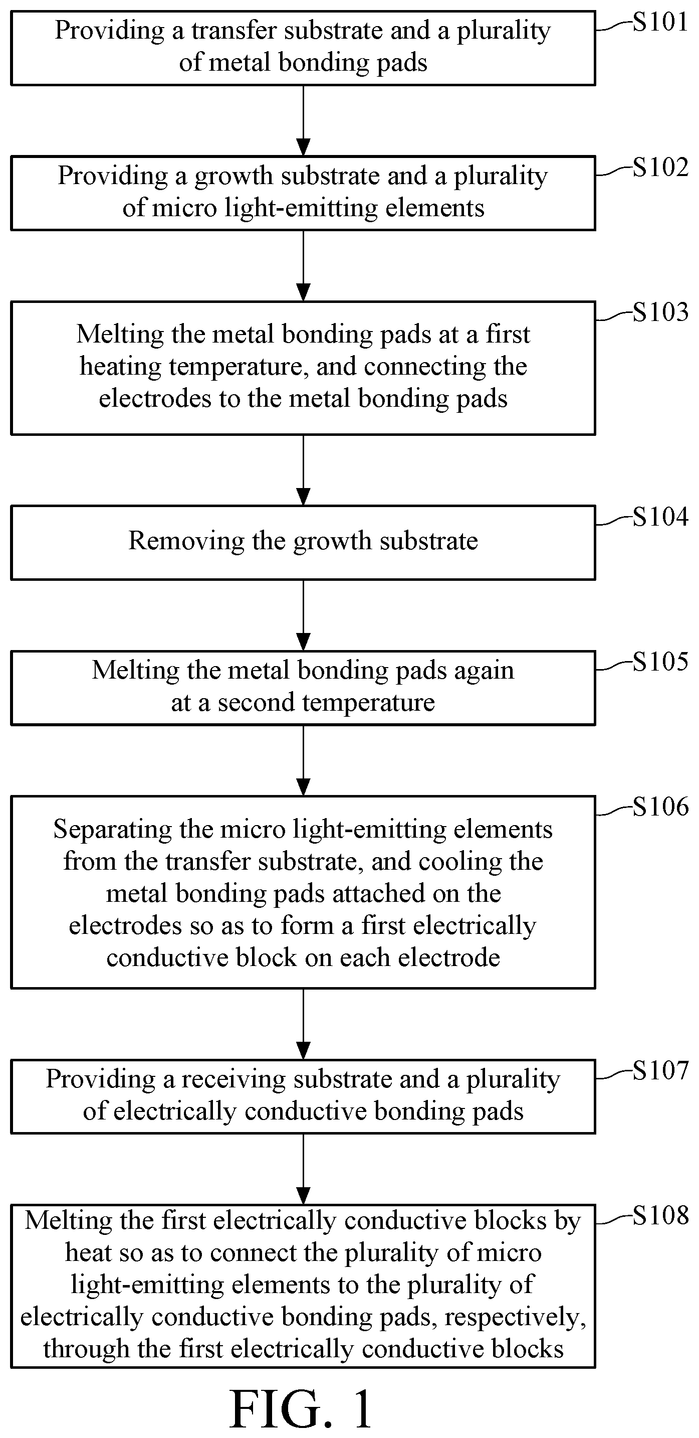
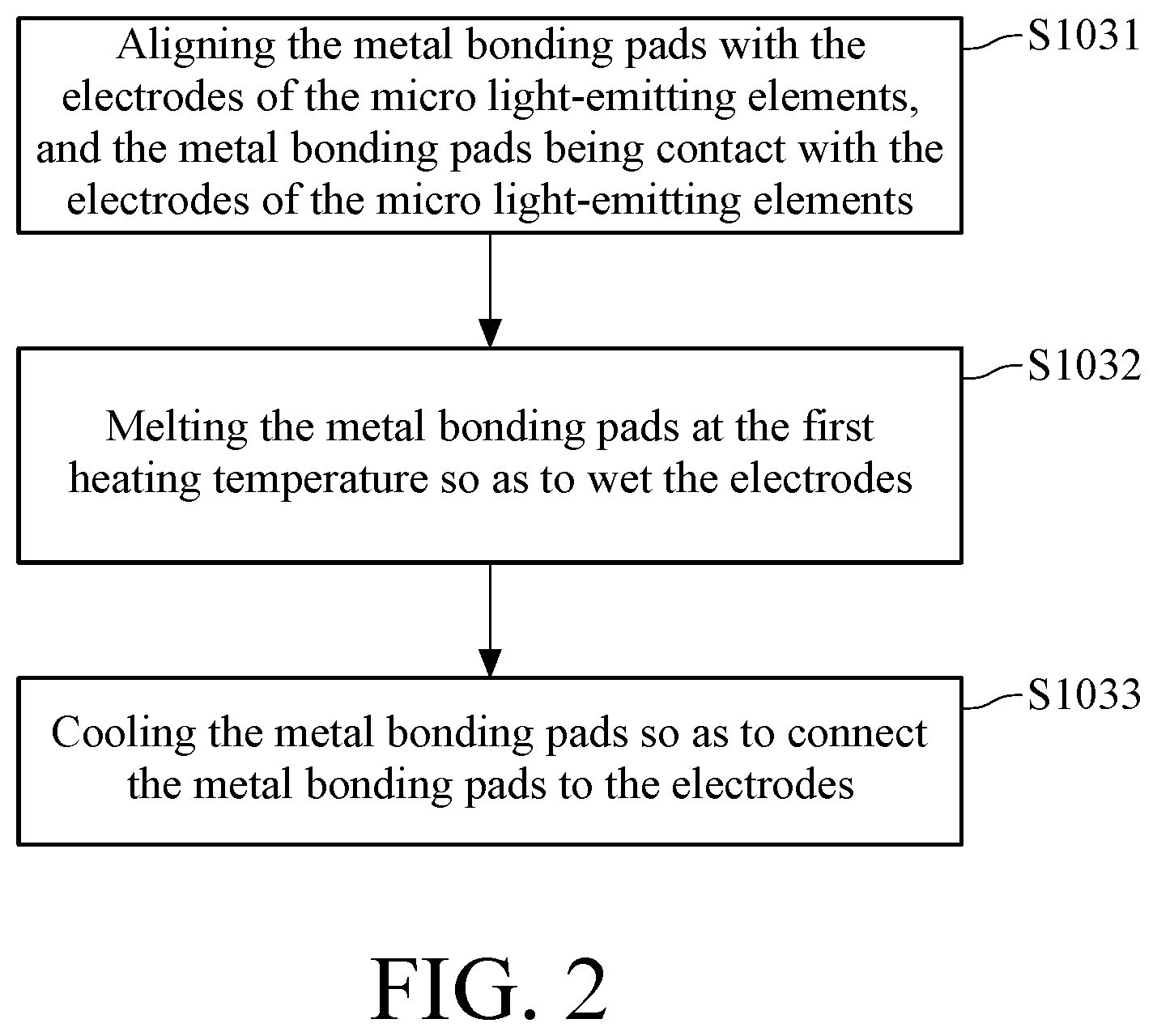
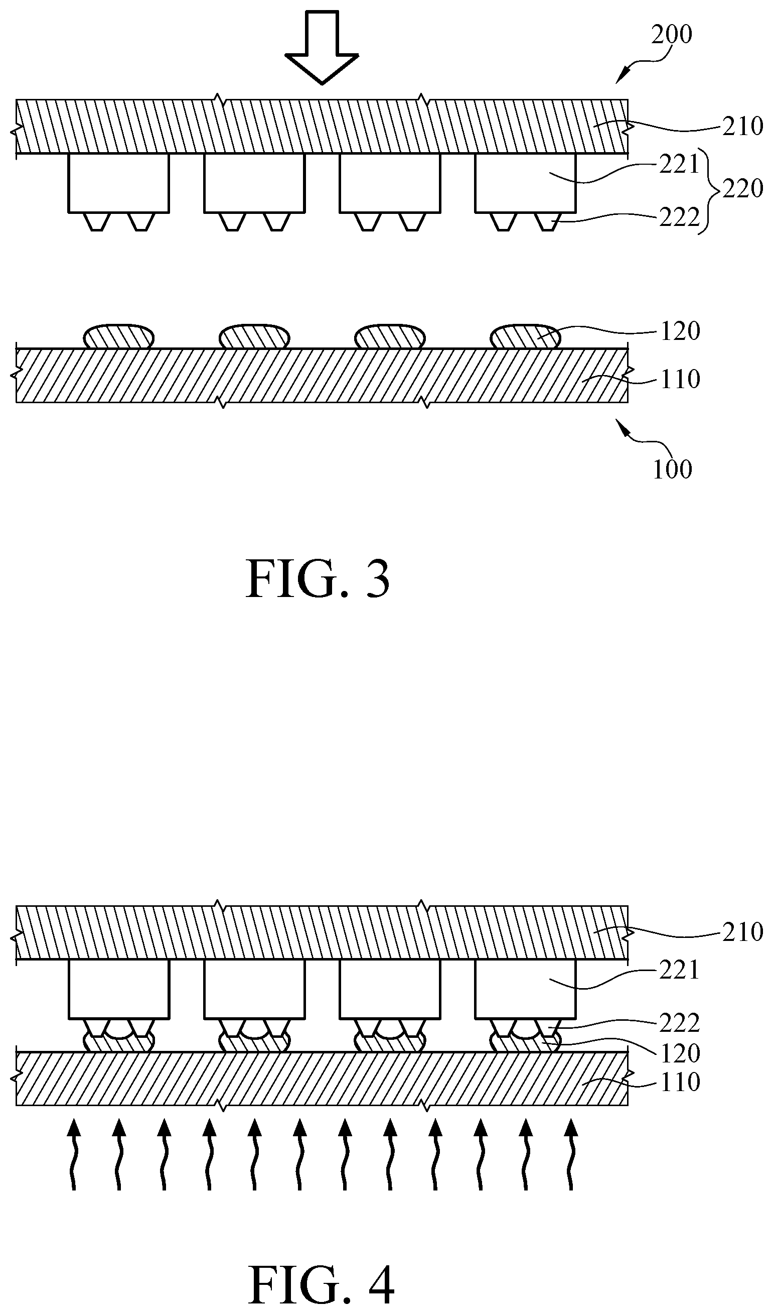
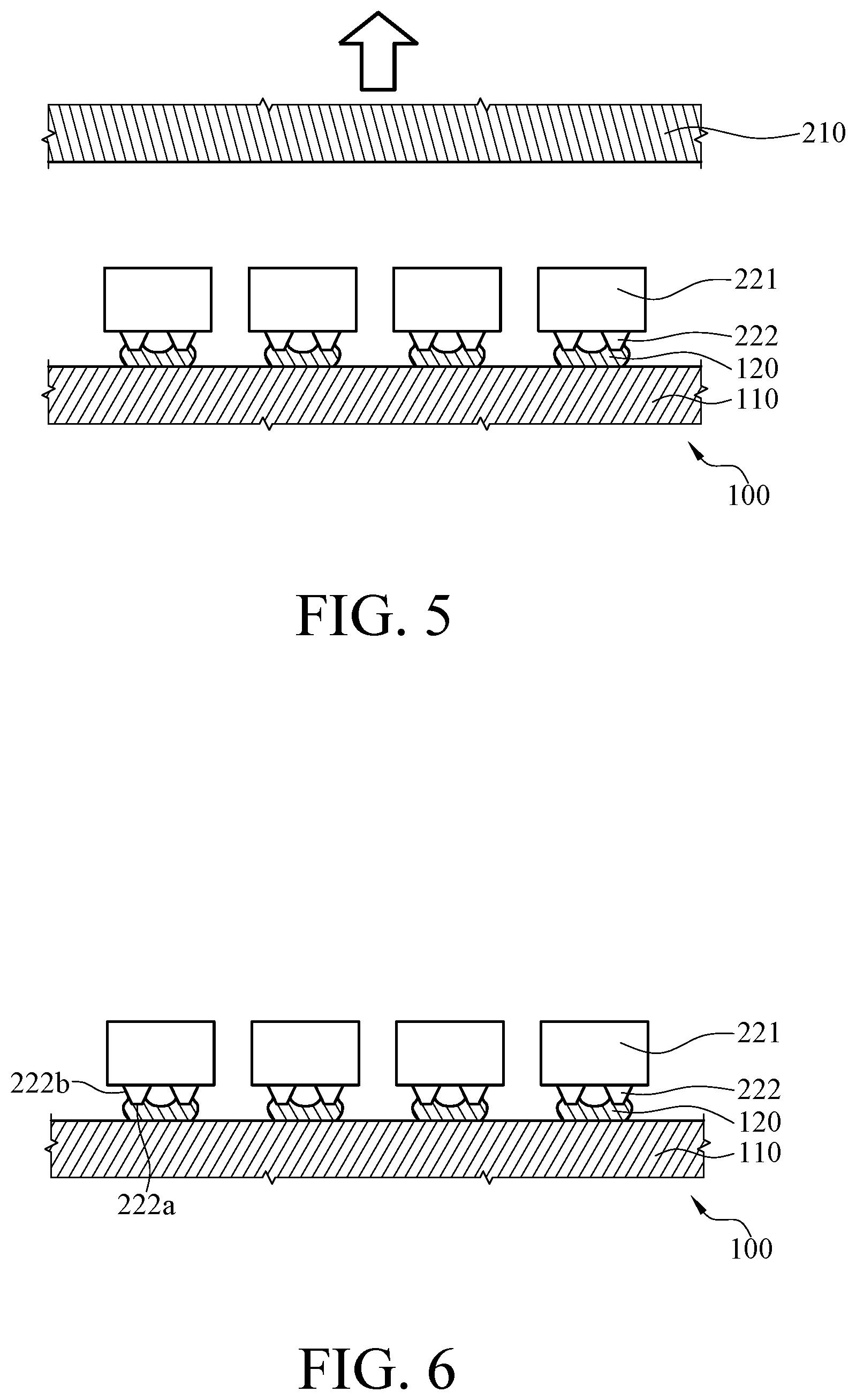
Method of manufacturing micro light-emitting element array, transfer carrier, and micro light-emitting element array
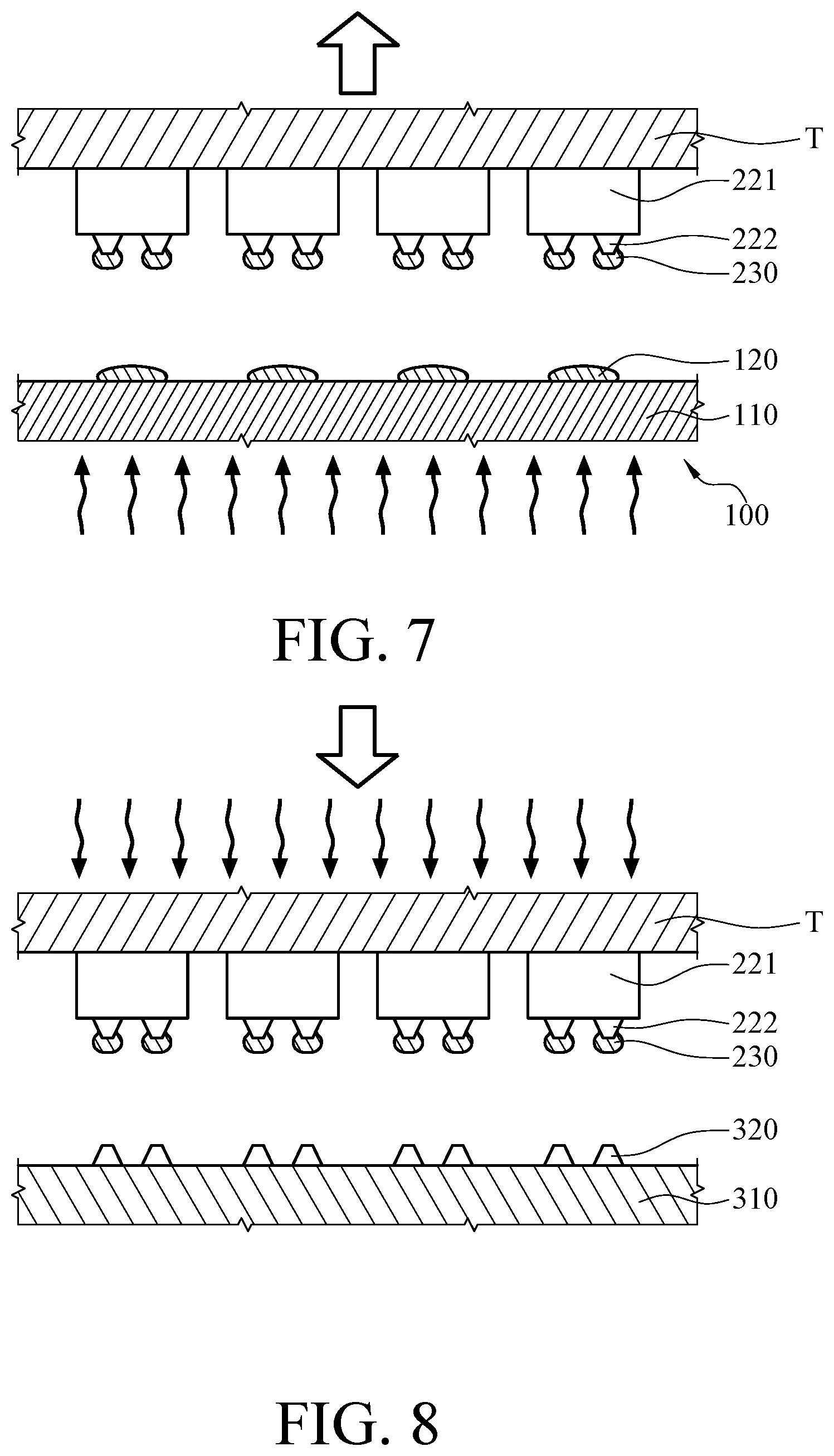
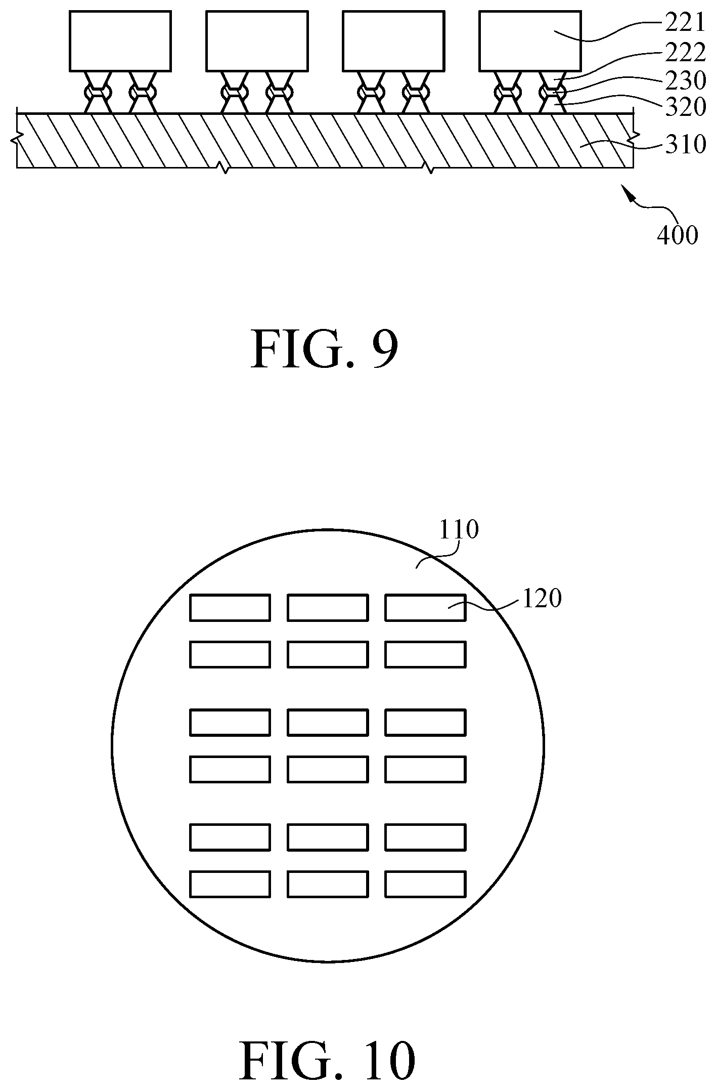
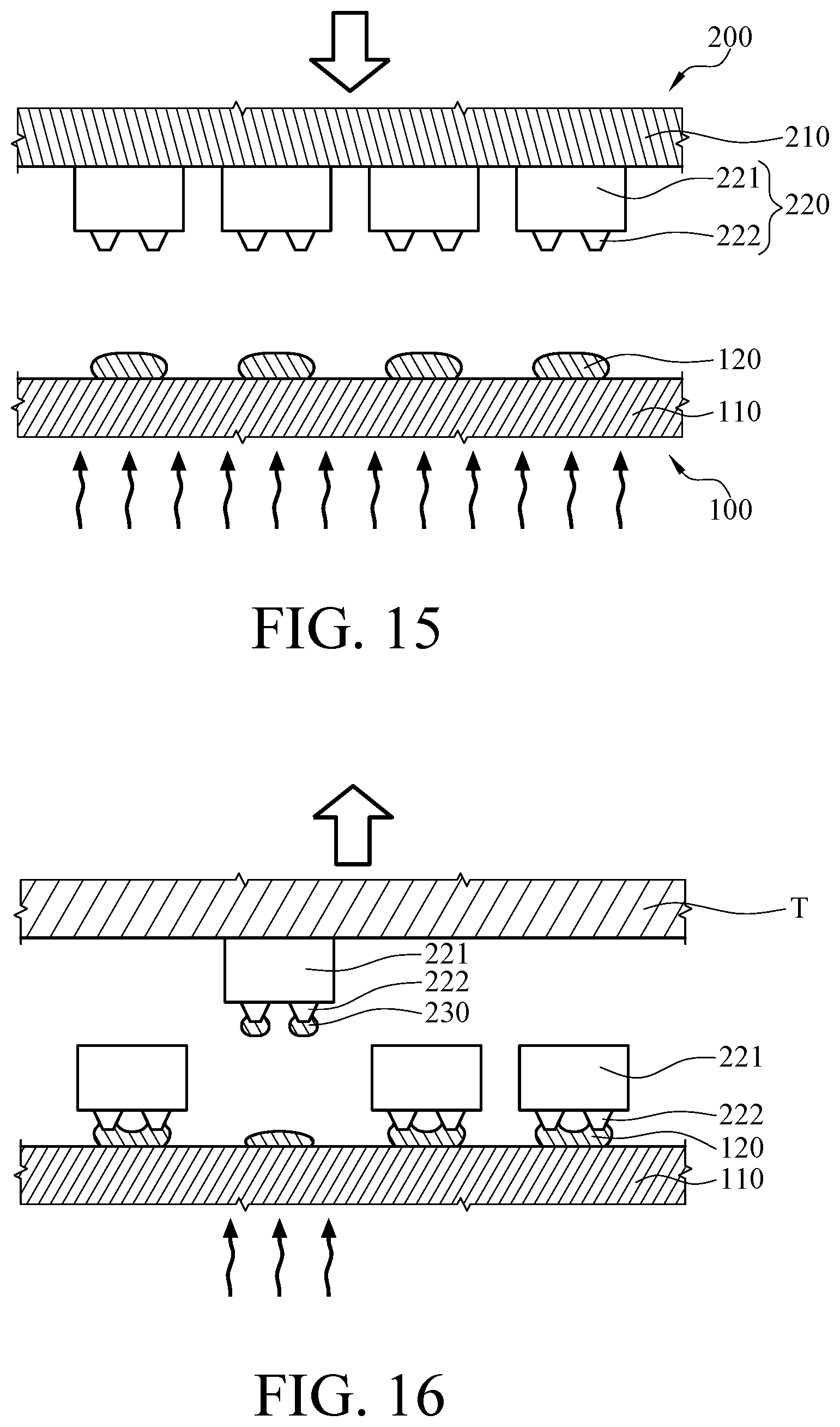
This non-provisional application claims priority under 35 U.S.C. § 119(a) on Patent Application No(s). 106131483 filed in Taiwan, R.O.C. on Sep. 13, 2017, the entire contents of which are hereby incorporated by reference. The disclosure relates to a method of manufacturing a micro light-emitting element array, a transfer carrier and a micro light-emitting element array, more particularly to a micro light-emitting element array, a transfer carrier and a micro light-emitting element array which are configured to simultaneously transfer the micro light-emitting element and dispose a first conductive bump. The light emitting diode (LED) is widely used in many fields as a light emitting element with high luminous efficiency. The conventional method of manufacturing the LED is the epitaxial method. An N-type semiconductor layer, a light emitting layer, and a P-type semiconductor layer are formed on a substrate in sequence so as to obtain the LED. When the size of the LED is reduced in micrometer scale, the LED is formed as a micro light-emitting element for a display device. In detail, a plurality of micro light emitting elements are arranged on a panel of the display device in an array arrangement so as to form a micro light-emitting element array used to be a light source of the display device which is known as the micro-LED display device. In the conventional method of manufacturing the display device, in order to transfer the micro light-emitting element array from an epitaxial substrate to the transfer substrate and then transfer the micro light-emitting element array from the transfer substrate to the panel, it is required to repeatedly attach bonding materials on the micro light-emitting element array, the transfer substrate and the panel. According to an embodiment of the present disclosure, a method of manufacturing micro light-emitting element array includes: providing a transfer substrate and at least one metal bonding pad, the metal bonding pad is disposed on the transfer substrate; providing a growth substrate and a plurality of micro light-emitting elements, the micro light-emitting elements are disposed on the growth substrate, and a surface of each of the micro light-emitting elements away from the growth substrate having at least one electrode; and melting the metal bonding pad at a heating temperature, and connecting the electrode to the metal bonding pad, and removing the growth substrate. According to another embodiment of the present disclosure, a transfer carrier is adapted to be connected to an electrode of a micro light-emitting element and transfer the micro light-emitting element. A transfer carrier includes a transfer substrate and a plurality of metal bonding pads. The metal bonding pads are disposed on the transfer substrate, and every two metal bonding pads that are adjacent to each other are spaced apart from each other through a gap. According to yet another embodiment of the present disclosure, a micro light-emitting element array includes a transfer carrier and a plurality of micro light-emitting elements. A transfer carrier includes a transfer substrate and at least one metal bonding pad. The metal bonding pad is disposed on the transfer substrate A surface of each of the micro light-emitting elements has at least one electrode. A connecting surface of the electrode and a lateral surface of the electrode are adjacent to each other. The metal bonding pad is connected to the connecting surface and a part of the lateral surface so as to fix the plurality of micro light-emitting elements on the transfer carrier. The present disclosure will become better understood from the detailed description given hereinbelow and the accompanying drawings which are given by way of illustration only and thus are not limitative of the present disclosure and wherein: FIG.1 is a flow chart of a method of manufacturing a micro light-emitting element array according to a first embodiment of the disclosure; In the following detailed description, for purposes of explanation, numerous specific details are set forth in order to provide a thorough understanding of the disclosed embodiments. It will be apparent, however, that one or more embodiments may be practiced without these specific details. In other instances, well-known structures and devices are schematically shown in order to simplify the drawing. The first embodiment of the present disclosure provides a method of manufacturing a micro light-emitting element array and a display device. Please refer to In the step S101, a transfer substrate and a plurality of metal bonding pads are provided. In detail, as shown in In the step S102, a growth substrate and a plurality of micro light-emitting elements are provided. In detail, as shown in In the first embodiment, it is noted that the thickness of the metal bonding pad 120 is from 3 μm to 4 μm, but the present disclosure is not limited thereto. In some other embodiment, the thickness of the metal bonding pad 120 may be from 1 μm to 6 μm. If the thickness of the metal bonding pad is greater than 6 μm, the molten metal bonding pad 120 may enter between and be connected to the two electrodes 222 when the molten metal pad 120 being connected to the micro light-emitting element 220 so as to cause a short circuit. If the thickness of the metal bonding pad is smaller than 1 μm, the contact area between the molten metal bonding pad 120 and the micro light-emitting element 220 may be insufficient when the molten metal pad 120 being connected to the micro light-emitting element 220 so as to cause a connection strength between the molten metal bonding pad 120 and the micro light-emitting element 220 being weak. The thickness of the epitaxial structure relates to a yield rate of the light-emitting element. In general, the thickness of the epitaxial structure is usually greater than 1 μm and preferably equal to 6 μm. A maximum width of the micro light-emitting element 220 is from 1 μm to 100 μm, preferably smaller than 30 μm. In the first embodiment, the maximum width of the micro light-emitting element 220 (e.g., Micro LED) is 1 μm. A peak value of the maximum current density of an external quantum efficiency curve of the micro light-emitting element 220 is from 0.01 A/cm2to 2 A/cm2. That is, the micro light-emitting element is adapted to operate in a low current density. In the step S103, the metal bonding pads are molten at a first heating temperature, and the electrodes of the micro light-emitting elements are connected to the metal bonding pads. In detail, as shown in In the sub-step S1031, the metal bonding pads are aligned and in contact with the electrodes of the micro light-emitting elements. In detail, the two electrodes 222 of each micro light-emitting element 220 are aligned with one of the metal bonding pads 120, and then the two electrodes 222 are contact with the corresponding metal bonding pad 120. If a single metal bonding pad 120 in plate shape or bar shape is provided, the metal bonding pad 120 is contact with a plurality of electrodes 222 of the micro light-emitting elements 220 in the same time. In some embodiments, when the metal bonding pads 120 are arranged in an array arrangement, the two electrodes 222 of each micro light-emitting element 220 are contact with one of the metal bonding pads 120. In the sub-step S1032, the metal bonding pads are molten at the first heating temperature, such that the electrodes of the micro light-emitting elements are wetted by the molten metal bonding pads. In detail, a melting point of the metal bonding pad 120 is smaller than a melting point of the electrode 222, and the first heating temperature is between the melting point of the metal bonding pad 120 and the melting point of the electrode 222. As such, when the metal bonding pad 120 on the transfer substrate 110 is heated at the first heating temperature, the metal bonding pad 120 is in a molten state, and the electrode 222 is still in a solid state. An intermolecular force between a molecule of the molten metal bonding pad 120 and a molecule of the electrode 222 is larger than an intermolecular force between molecules of the molten metal bonding pad 120 such that the molten metal bonding pad 120 wets the electrode 222. Because the metal bonding pad 120 has lower melting point, melting the metal bonding pad 120 does not require too high heating temperature, thereby decreasing the difficulty in the manufacturing process, and preventing the micro light-emitting element and other elements from broken. In the first embodiment, the metal bonding pad 120 is heated, for example, by laser. In the sub-step S1033, the molten metal bonding pads are cooled down such that the metal bonding pads are connected to the electrodes. In detail, after the metal bonding pads 120 are stopped being heated, the metal bonding pads 120 are cooled and solidified. As such, each solidified metal bonding pad 120 is connected to the two electrodes 222 of each micro light-emitting element 220 so as to connect each micro light-emitting element 220 to the transfer substrate 110. In the first embodiment, the first heating temperature is also smaller than a eutectic temperature of a eutectic bonding between the metal bonding pad 120 and the electrode 222. For example, the first heating temperature may be equal to either a peritectic temperature of a peritectic reaction between the metal bonding pad 120 and the electrode 222, the melting point of the metal bonding pad or a temperature slightly higher than the melting point of the metal bonding pad. The first heating temperature is smaller than the eutectic temperature. Therefore, in the first embodiment, a contact surface between the metal bonding pad 120 and the electrode 222 is in a non-wetting state. The connection between the metal bonding pad 120 and the electrode 222 is relied on a physical or chemical diffusion force instead of a bonding force produced by the eutectic bonding. In the step S104, the growth substrate is removed. In detail, as shown in According to the aforementioned steps S101 to step S104, the micro light-emitting element array can be obtained. As shown in In the first embodiment, the ratio of an area of the lateral surface 222 Comparing the metal bonding pad 120 being glued on the electrode 222, when the metal bonding pad 120 is connected to the electrode 222 through a peritectic reaction or the diffusion force of the non-wetting state, the connection strength between the metal bonding pad 120 and the electrode 222 is much stronger. As such, during the transfer of the micro light-emitting elements 220, any unexpected shift in position of each micro light-emitting element 220 is prevented. After removing the growth substrate to obtain the micro light-emitting element array, the micro light-emitting elements 220 of the micro light-emitting element array are able to be transferred to a receiving substrate 310 so as to be convenient for manufacturing a display device 400 including the receiving substrate 310 and the micro light-emitting elements 220. The method of transferring the micro light-emitting elements of the micro light-emitting element array to the receiving substrate is illustrated in the following paragraphs. In the step S105, the metal bonding pads are molten again at a second heating temperature. In detail, as shown in In the step S106, the micro light-emitting elements are separated from the transfer substrate, and a part of each molten metal bonding pad is attached on each electrode, and the metal bonding pads are cooled down so as to form a first conductive bump on each electrode. In detail, as shown in In the first embodiment, the peritectic reaction and the non-wetting state between the metal bonding pad 120 and the electrode 222 are reversible. Therefore, in the process of transferring the micro light-emitting element 220 to the receiving substrate 310, the second heating temperature in removing the peritectic reaction or the non-wetting state is smaller than a heating temperature in removing the eutectic bonding, thereby preventing the micro light-emitting element 220 from being broken. In the step S107, the receiving substrate and a plurality of conductive bonding pads are provided. In detail, as shown in The receiving substrate 310 is, for example, a complementary metal-oxide-semiconductor substrate, a printed-circuit board, a liquid crystal on silicon substrate, a thin-film transistor substrate and so on. The material of the conductive bonding pad 320 is, for example, Ti, Pt, Au, Al, Ni, Cr or an alloy of above metal. In the step S108, the first conductive bumps are molten by heat such that the first conductive bumps are respectively connected to the conductive bonding pads disposed on the receiving substrate. In detail, as shown in As shown in In the first embodiment, the temperature of the molten first conductive bump 230 is not only larger than a eutectic temperature between the first conductive bump 230 and the electrode 222, but also larger than a eutectic temperature between the first conductive bump 230 and the conductive bonding pad 320. Accordingly, the first conductive bump 230 and the conductive bonding pad 320 are in eutectic bonding, and the first conductive bump 230 and the electrode 222 are in eutectic bonding such that the micro light-emitting element 220 is firmly fixed on the receiving substrate 310. In the first embodiment, before the micro light-emitting element 220 is connected to the conductive bonding pad 320, the peritectic reaction between the first conductive bump 230 and the electrode 222 produces delicate alloy grains inside or on a surface of the first conductive bump 230. When the first conductive bump 230 having the delicate alloy grains and the conductive bonding pad 320 are in the eutectic bonding, the delicate grains increase the connection quality between each other so as to provide a better connection strength or reduce the resistance between them. In the first embodiment, there is no any second conductive bump disposed on the surface of the conductive bonding pad 320, but the present disclosure is not limited thereto. In the first embodiment, there may be another type of the receiving substrate 310 and the conductive bonding pad 320. Please refer to In the first embodiment, when the transfer carrier 100 is separated from the micro light-emitting element 220, a part of the metal bonding pad 120 is attached on the micro light-emitting element 220. As such, the metal bonding pad 120 attached on the micro light-emitting element 220 can be taken as the first conductive bump 230 for connecting the micro light-emitting element 220 to the receiving substrate 310, thereby decreasing the frequency in disposing the bonding material and the cost of manufacturing the display device, and increasing the reliability of the display device. The following paragraphs will illustrate a second embodiment of the disclosure. Please refer to In the first embodiment, the step S103 includes melting the metal bonding pad at a first heating temperature, and connecting the electrode of the micro light-emitting element to the metal bonding pad. The step S103 includes the sub-step S1031, S1032 and S1033. The sub-step S1031 includes aligning the metal bonding pad with the electrode of the micro light-emitting element, and the metal bonding pad being in contact with the micro light-emitting element. The sub-step S1032 includes melting the metal bonding pad at the first heating temperature so as to wet the electrode by the molten metal bonding pad. The sub-step S1033 includes cooling the molten metal bonding pad so as to connect the metal bonding pad to the electrode. In the second embodiment, a step includes sub-steps S2031, S2032 and S2033 which are respectively different from the sub-steps S1031, S1032 and S1033. The following paragraphs will illustrate the sub-steps S2031, S2032 and S2033. In the sub-step S2031, a metal bonding pad is molten at a third heating temperature. In detail, as shown In the sub-step S2032, the molten metal bonding pad is aligned with the electrode of the micro light-emitting element, and the molten metal bonding pad is in contact with the electrode of the micro light-emitting element so as to wet the electrode. In detail, the electrode 222 of each micro light-emitting element 220 is aimed to the molten metal bonding pad 120, and then the electrode 222 of each micro light-emitting element 220 is in contact with the metal bonding pad 120. If the metal bonding pad 120 is a single pad in plate shape or in bar shape, the metal bonding pad 120 is in contact with a plurality of electrodes 222 of the micro light-emitting elements 220 in the same time. If the metal bonding pad 120 is one of pads which are arranged in an array arrangement, the metal bonding pad 120 is only in contact with the electrode 222 of one micro light-emitting element 220. An intermolecular force between a molecule of the molten metal bonding pad 120 and a molecule of the electrode 222 is larger than an intermolecular force between molecules of the molten metal bonding pad 120 such that the molten metal bonding pad 120 wets the electrode 222 and attaches on the electrode 222. In the step S2033, the molten metal bonding pad is cooled down so as to connect the metal bonding pad to the electrode. In detail, after the metal bonding pad 120 is connected to the electrode 222, the molten metal bonding pad 120 is cooled down and solidified. As such, the solidified metal bonding pad 120 is connected to the electrode 222 so as to connect the micro light-emitting element 220 to the transfer substrate 110. In the second embodiment, the requirement of the third heating temperature is similar to the requirement of the first heat temperature in the first embodiment, thus the following paragraphs will not further illustrate. Then, the following paragraphs illustrate a micro light-emitting element array of the disclosure in an application of repairing a defective pixel of the display device. Please refer to In a manufacturing process of the display device, the micro light-emitting element array on the receiving substrate 310 are required to be tested so as to ensure that each micro light-emitting element 220 can normally emit light. When a micro light-emitting element 220 is failed, it is necessary to replace the failed micro light-emitting element 220. First, the failed micro light-emitting element (not shown in figures) is removed from the receiving substrate 310. Then, a specific area of the micro light-emitting element array shown in The following paragraphs will illustrate a transfer carrier of each of a third embodiment to a sixth embodiment. Please refer to A transfer carrier 100 The under-bump metal structure 130 is wettable to the molten metal bonding pad 120. The barrier layer 140 is non-wettable to the molten metal bonding pad 120. As such, in the manufacturing process of the transfer carrier 100 In the transfer carrier 100 A transfer carrier 100 The partitioning material 150 is non-wettable to the molten metal bonding pad 120. The wetting layer 160 is wettable to the molten metal bonding pad 120. As such, in the manufacturing process of the transfer carrier 100 In the transfer carrier 100 A transfer carrier 100 The barrier layer 140 is wettable to the molten metal bonding pad 120. The partitioning material 150 is non-wettable to the molten metal bonding pad 120. As, such, in the manufacturing process of the transfer carrier 100 In the transfer carrier 100 In the process of connecting the electrode 222 of the micro light-emitting element 220 to the metal bonding pad 120 of the transfer carrier 100 The transfer carrier 100 In the sixth embodiment, the material of the wetting layer 160 is, for example, Ti, Pt, Au, Al, Ni, Cr or an alloy of above metal. According to the method of manufacturing the micro light-emitting element array, the transfer carrier and the micro light-emitting element array as discussed above, when the transfer carrier is separated from the micro light-emitting element, a part of the metal bonding pad is attached on the micro light-emitting element. As such, the metal bonding pad attached on the micro light-emitting element can be taken as the first conductive bump for connecting the micro light-emitting element to the receiving substrate, thereby decreasing the frequency in disposing the bonding material and the cost of manufacturing the display device, and increasing the reliability of the display device. A method of manufacturing micro light-emitting element array is disclosed. A transfer substrate and at least one metal bonding pad are provided, and the metal bonding pad is disposed on the transfer substrate. A growth substrate and a plurality of micro light-emitting elements are provided. The micro light-emitting elements are disposed on the growth substrate, and a surface of each of the micro light-emitting elements away from the growth substrate having at least one electrode. The metal bonding pad is molten at a heating temperature, and the electrode is connected to the metal bonding pad. Then, the growth substrate is removed. 1. A method of manufacturing micro light-emitting element array, comprising:
providing a transfer substrate and at least one metal bonding pad, wherein the at least one metal bonding pad is disposed on the transfer substrate; providing a growth substrate and a plurality of micro light-emitting elements, wherein the plurality of micro light-emitting elements are disposed on the growth substrate, and a surface of each of the plurality of micro light-emitting elements away from the growth substrate having at least one electrode, the at least one electrode having a connecting surface and a lateral surface adjacent to each other; melting the at least one metal bonding pad at a heating temperature, wherein the heating temperature is smaller than an eutectic temperature of eutectic bonding between the at least one metal bonding pad and the at least one electrode; connecting the at least one electrode to the at least one metal bonding pad, wherein the at least one metal bonding pad is connected to the connecting surface of the at least one electrode through a diffusion force, the connection between the at least one metal bonding pad and the connecting surface of the at least one electrode is achieved by peritectic reaction or in a non-wetting state, and the connection is reversible, and a ratio of an area of the lateral surface covered by the at least one metal bonding pad to a surface area of the lateral surface is greater than or equal to 0.05 and is smaller than or equal to 0.3; removing the growth substrate; melting the at least one metal bonding pad again; and separating the plurality of micro light-emitting elements from the transfer substrate, wherein a part of the at least one metal bonding pad is attached on the at least one electrode, and the part of the at least one metal bonding pad attached on the at least one electrode is cooled down so as to form a first conductive bump. 2. The method according to aligning the at least one metal bonding pad with the at least one electrode, and the at least one metal bonding pad being in contact with the at least one electrode; melting the at least one metal bonding pad at the heating temperature so as to wet the at least one electrode by the at least one metal bonding pad which is molten; and cooling the at least one metal bonding pad so as to connect the at least one metal bonding pad to the at least one electrode. 3. The method according to melting the at least one metal bonding pad at the heating temperature; aligning the at least one metal bonding pad, which is molten, with the at least one electrode, and the at least one metal bonding pad being in contact with the at least one electrode so as to wet the at least one electrode by the at least one metal bonding pad; and cooling the at least one metal bonding pad so as to connect the at least one metal bonding pad to the at least one electrode. 4. The method according to 5. The method according to 6. The method according to 7. The method according to 8. The method according to 9. The method according to 10. The method according to 11. The method according to providing a receiving substrate and a plurality of conductive bonding pads, wherein the plurality of conductive bonding pads are disposed on the receiving substrate in array arrangement; and melting the first conductive bump by heat so as to connect the plurality of micro light-emitting elements to the plurality of conductive bonding pads, respectively, through the first conductive bump. 12. The method according to 13. The method according to 14. The method according to 15. The method according to 16. A micro light-emitting element array, comprising:
a transfer carrier comprising a transfer substrate and at least one metal bonding pad, and the at least one metal bonding pad being disposed on the transfer substrate; and a plurality of micro light-emitting elements, a surface of each of the plurality of micro light-emitting elements having at least one electrode, a connecting surface of the at least one electrode and a lateral surface of the at least one electrode being adjacent to each other, and the at least one metal bonding pad is connected to the connecting surface and a part of the lateral surface so as to fix the plurality of micro light-emitting elements on the transfer carrier; wherein the at least one metal bonding pad is connected to the connecting surface of the at least one electrode through a diffusion force, the connection between the at least one metal bonding pad and the connecting surface of the at least one electrode is achieved by peritectic reaction or in a non-wetting state, and the connection is reversible, and a ratio of an area of the lateral surface covered by the at least one metal bonding pad to a surface area of the lateral surface is greater than or equal to 0.05 and is smaller than or equal to 0.3.CROSS-REFERENCE TO RELATED APPLICATIONS
TECHNICAL FIELD
BACKGROUND
SUMMARY
BRIEF DESCRIPTION OF THE DRAWINGS
DETAILED DESCRIPTION


CPC - классификация
HH0H01H01LH01L2H01L21H01L21/H01L21/6H01L21/68H01L21/683H01L21/6835H01L22H01L222H01L2221H01L2221/H01L2221/6H01L2221/68H01L2221/683H01L2221/6835H01L2221/68354H01L2221/6836H01L2221/68368H01L2224H01L2224/H01L2224/1H01L2224/11H01L2224/110H01L2224/1100H01L2224/11001H01L2224/114H01L2224/1142H01L2224/11422H01L2224/13H01L2224/130H01L2224/1308H01L2224/13082H01L2224/131H01L2224/1312H01L2224/13124H01L2224/1313H01L2224/13139H01L2224/1314H01L2224/13144H01L2224/13147H01L2224/1315H01L2224/13155H01L2224/1316H01L2224/13166H01L2224/8H01L2224/81H01L2224/810H01L2224/8100H01L2224/81005H01L2224/811H01L2224/8119H01L2224/81193H01L2224/818H01L2224/8181H01L2224/81815H01L2224/9H01L2224/95H01L24H01L24/H01L24/0H01L24/03H01L24/1H01L24/11H01L24/13H01L24/8H01L24/81H01L24/9H01L24/95H01L25H01L25/H01L25/0H01L25/07H01L25/075H01L25/0753H01L25/5H01L25/50H01L27H01L27/H01L27/1H01L27/15H01L27/156H01L29H01L292H01L2924H01L2924/H01L2924/0H01L2924/00H01L2924/000H01L2924/0001H01L2924/00014H01L2924/1H01L2924/12H01L2924/120H01L2924/1204H01L2924/12041H01L3H01L33H01L33/H01L33/0H01L33/00H01L33/005H01L33/009H01L33/0093IPC - классификация
HH0H01H01LH01L2H01L21H01L21/H01L21/6H01L21/68H01L21/683H01L23H01L23/H01L23/0H01L23/00H01L25H01L25/H01L25/0H01L25/00H01L25/07H01L25/075H01L27H01L27/H01L27/1H01L27/15H01L3H01L33H01L33/H01L33/0H01L33/00Цитирование НПИ
29/832438/107
438/121
438/27
CRC Handbook of Chemistry and Physics, pp. 4-121˜123 (Year: 2016).
Jet Process Corporation: AuSb Pb Free Solders (http://www.jetprocess.conn/solder-coatings/ausn-pb-free-solders), archived 2015 (Year: 2016).
Kim et al., Fluxless silicon-to-alumina bonding using electroplated Au—Sn—Au structure at eutectic composition, Materials Science and Engineering A 458 (2007) 101-107 (Year: 2007).