DIE BONDING TO A BOARD
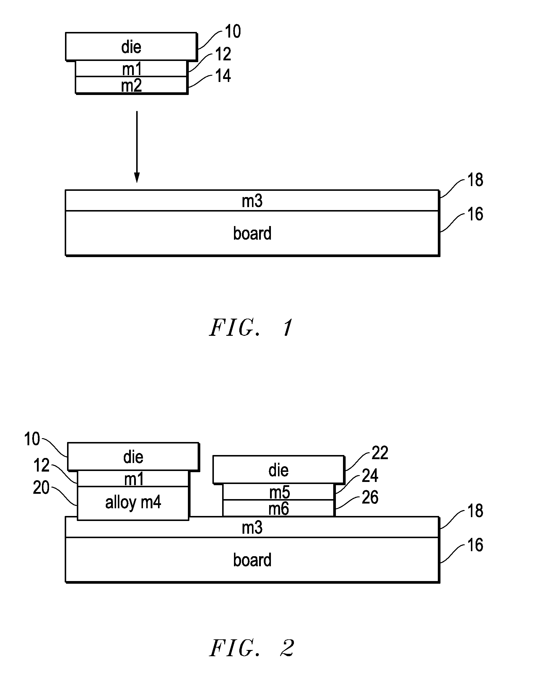
This application is a division of U.S. patent application Ser. No. 14/812,846, filed Jul. 29, 2015, entitled “Die Bonding to a Board,” invented by Michael J. Seddon et al., and claims priority to U.S. Provisional Application No. 62/194,204, filed Jul. 18, 2015, invented by Michael J. Seddon et al., the contents of which are incorporated herein by reference in their entirety. The present disclosure relates generally to circuit manufacturing, and more particularly to device bonding techniques. Multichip modules are increasingly being used to control operations of machines and systems. For a variety of manufacturing considerations, however, the various devices are not always installed into the multichip modules at the same time. Wire bond applications are often used though not always appropriate for certain applications. For example, a wire bond solution may not be appropriate in situations where footprint requirements necessitate efficient integrated circuit (IC) real estate usage. An alternative approach is to use solder alloys and pastes. Using solder in either form is beneficial for bonding one die to a board, such as a ceramic or substrate board or metal lead frame, in certain circumstances. Typically, the solder alloy or paste will flow when the device and board are placed in a reflow oven or furnace and will then cool to bond the die to the board and, if desired, to create an electrical connection between the device and board. For the case of a single die, this approach is beneficial in that the die may be removed and replaced if faulty with a subsequent reflow in a reflow oven or furnace. One issue with using a solder alloy or paste, however, is that the solder will reflow and the bond between the original die and the board will fail when the board and a new die are subsequently placed in the reflow oven to bond the new die to the board. When the bond fails, the original die may even slide off of the board or metal lead frame. One approach to solve this problem has been to use different metal alloys for the original or first die so that the metal alloys bonding the die have a higher melting temperature than what is needed for re-flowing the solder alloys of the second or new die. Two metals that have been used with this approach include lead and gold. Lead, however, is known to cause health issues and is not always desirable. Gold, on the other hand, is expensive and drives up product cost. Accordingly, solder is often used despite its limitations. The present disclosure may be better understood, and its numerous features and advantages made apparent to those skilled in the art by referencing the accompanying drawings according to various embodiments in which: The use of the same reference symbols in different drawings indicates similar or identical items. Unless otherwise noted, the word “coupled” and its associated verb forms include both direct connection and indirect electrical connection by means known in the art, and unless otherwise noted any description of direct connection implies alternate embodiments using suitable forms of indirect electrical connection as well. Metal layer 18 of board 16 comprises at least one of a solderable metal layer such tin, silver or copper. Metal layer 18 may also comprise a plurality of metal or metal alloy layers, for example, copper, nickel, tin or silver or an alloy formed of two or more metals. The metal layers on the die comprise a combination of silver, tin and nickel in one embodiment. The die may include three or more layers. While As is suggested in Here, in In one embodiment of the invention, a process includes reflowing a die until at least two metals melt and mix to create an alloy. As an additional process step, the reflow may be extended in time to a second period to cause at least a third metal, if not a fourth metal, of either a die layer or a board layer to mix to create additional alloys. It should be understood that distinct layers are shown here to represent alloys with differing combinations of metal. In actual practice, however, the ratios of metal may gradually change depending on original metal layer thicknesses and a total period of the reflow process to create the alloys. Accordingly, it should be understood that the term “intermetallic alloy” or “intermetallics” may be used in place of alloy more appropriately depending on the results of the reflow process. Reflow duration and relative layer thickness and construction affect how much the various metal layers melt and how well they mix to create a uniform distribution of metals within the resulting alloy. For example, if the metal compositions are different in different areas, the term “intermetallic alloy” may be more appropriate than the term “alloy” because “alloy” tends to refer to a homogenous or uniform distribution of metal content. References herein to alloy are intended to include intermetallic alloys. Time t0 is the time at which the reflow temperature is reached while time t1 is an amount of time that is required to form an alloy and create a bond. Time t1 may coincident with time t0. Time t1 is a function of what metals are being melted and the relative thickness of the metal layers. Furthermore, as described in relation to previous figures, a plurality of metal layers may be used on at least one of the die or the board. If the reflow temperature is maintained beyond time t1 to time t2, additional alloys may be formed from the additional metal layers disposed either on the die or on the board because maintaining the reflow temperature causes additional melting. Accordingly, shortly after time t2, period 5 begins representing a cool down period. As described before, the alloys that are formed by the reflow temperature at times t1 and t2 have subsequent melting temperatures that are higher than the reflow temperature of period p4. The process represented by The temperature profile may include a temperature ramp to a specified temperature with an immediate cool down following or a ramp to a temperature or temperature range that is maintained for a specified period or duration sufficient to allow the metal layers to reflow to create at least one alloy. Reference herein to temperature profiles include any combination of temperature and time that is used to melt the die and board metal layers to create the desired alloys and/or intermetallic alloys. The method optionally includes continuing the reflow according to a second temperature profile (e.g. at the first reflow temperature profile for a second period) to continue to reflow the first die and one or more of the metal layers of the die and the board to form a second alloy or intermetallic alloy (108). After a first reflow process is concluded and any formed alloys have cooled and hardened, the method includes placing a second die on the solderable board (110) board with the first and second die in the reflow furnace or oven (112) to essentially repeat the reflow process. Thereafter, second die and board metal layers are reflowed according to a third reflow temperature profile without completely re-flowing any alloy metals of the first die and board that were created during the first reflow process. The second die and board metal layers are re-flowed to form a third alloy for the second die and board (114). Finally, the method optionally includes continuing to reflow the metal layers of the second die and board according to a fourth temperature profile to form a fourth alloy for the second die (116). It should be understood that the first, second, third and fourth temperature profiles may be similar or may be varied in thickness or composition. Similarly, the first, second, third and fourth alloys and/or intermetallics that are created are based on the temperature profiles and metal layer compositions and may therefore be similar or different. Optionally, the board and die are kept at the second temperature for a specified period. The method continues with continuing to maintain heat to continue to reflow the board metal with first and second die metal layers to form a second alloy (126). This step includes maintaining a specified temperature range (e.g., the second temperature reached in step 124) for a specified period. In the described embodiment, a solder or solder paste was not used. Alternatively, for the method of After the first and second alloys have cooled enough to bond the die to the board, the method includes placing a second die against the board without solderable paste (128). Thereafter, the method optionally includes heating the second die and the board with the attached first die to the first temperature to burn off flux and/or impurities (130). Thereafter, the reflow oven or furnace temperature is increased to heat the board according to a fourth temperature to reflow the board metal layer and the second die first metal layer to form a third alloy (132). As described in relation to step 124, the fourth temperature may be the same as the second temperature or it may be modified according to design requirements. Finally the method concludes with maintaining the heat at the fourth temperature or within a temperature range approximately equal to the fourth temperature to reflow the board metal layer with the second die first and second die metal layers to form a fourth alloy (134). As before, this step may comprise merely maintaining a specified temperature or temperature range for a specified period. It should be understood that the first and second die might have substantially similar metal layers thereby resulting in substantially similar alloys from the reflow processes. In other words, the third and fourth alloys may be very similar to the first and second alloys, respectively if the metals and temperature profiles or processes are similar. The above-disclosed subject matter is to be considered illustrative, and not restrictive, and the appended claims are intended to cover all such modifications, enhancements, and other embodiments that fall within the true scope of the claims Thus, to the maximum extent allowed by law, the scope of the present invention is to be determined by the broadest permissible interpretation of the following claims and their equivalents, and shall not be restricted or limited by the foregoing detailed description. An apparatus for bonding die to a board includes a circuit board having a solderable layer and a plurality of die bonded to the circuit board using at least three respective layers. Each of the at least three respective layers includes an inner layer, a first alloy of material from an outer layer and the solderable layer of the circuit board, and a second alloy of material from the outer layer and the solderable layer of the circuit board. Melting temperatures of the first alloy and the second alloy are higher than reflow temperatures of the outer layer and the solderable layer of the circuit board. 1. An apparatus, comprising:
a first solderable layer on a surface of a ceramic or substrate board or a metal lead frame; first circuitry comprising:
a first solderable die surface on a first die comprising a first plurality of metal layers wherein an outer layer comprises a silver and tin first alloy having a silver composition that is less than 7 percent by weight and wherein an inner layer next to the outer layer comprises one of titanium, nickel or silver; and a second alloy having a subsequent melting temperature that is higher than a first reflow temperature required to adhere the first die to the first solderable layer of the board, wherein the second alloy bonds the first alloy to the first solderable layer of the surface of the board to hold the first die to the board, and second circuitry comprising:
a second solderable die surface on a second die comprising a third alloy, wherein the first and second circuitry are configured to control operations of the apparatus. 2. The apparatus of 3. The apparatus of 4. The apparatus of 5. The apparatus of the first reflow temperature is in a range of from 220 degrees C. to 260 degrees C.; and the subsequent melting temperature of the second alloy is higher than 260 degrees C. 6. An apparatus, comprising:
a circuit board having a solderable layer; a plurality of die bonded to the circuit board using at least three respective layers, each of the at least three respective layers comprising:
an inner layer; a first alloy of material from an outer layer and the solderable layer of the circuit board; and a second alloy of material from the outer layer and the solderable layer of the circuit board, wherein melting temperatures of the first alloy and the second alloy are higher than reflow temperatures of the outer layer and the solderable layer of the circuit board. 7. The apparatus of the circuit board comprises a ceramic board. 8. The apparatus of the circuit board comprises a metal lead frame. 9. The apparatus of the inner layer of the at least three respective layers comprises silver. 10. The apparatus of the outer layer comprises tin. 11. The apparatus of the first alloy comprises an alloy of silver and tin. 12. The apparatus of the solderable layer of the circuit board comprises at least one of copper, nickel, tin, and silver. 13. The apparatus of the solderable layer of the circuit board comprises a metallic layer of one of copper, tin, and silver. 14. The apparatus of the solderable layer of the circuit board comprises an alloy formed of two or more metals. 15. The apparatus of the melting temperatures of the first alloy and the second alloy are at least 15 degrees C. higher than the reflow temperatures of the inner layer and the outer layer. 16. The apparatus of the reflow temperatures of the inner layer and the outer layer are in a range of from 220 degrees C. to 260 degrees C.; and the melting temperatures of the first alloy and the second alloy are higher than 260 degrees C. 17. The apparatus of the solderable layer of the circuit board comprises copper. 18. The apparatus of the solderable layer of the circuit board comprises a plurality of layers. 19. The apparatus of the plurality of layers of the solderable layer of the circuit board comprise at least one metal layer. 20. The apparatus of the plurality of layers of the solderable layer of the circuit board comprise at least one metal alloy layer.CROSS-REFERENCE TO RELATED APPLICATIONS
FIELD OF THE DISCLOSURE
BACKGROUND
BRIEF DESCRIPTION OF THE DRAWINGS
DETAILED DESCRIPTION