Molded die last chip combination
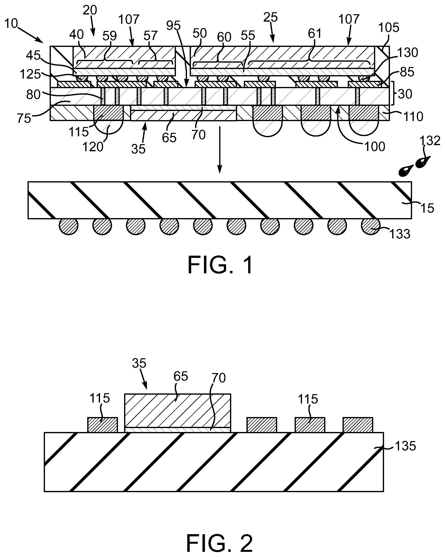
A conventional type of multi-chip module includes two semiconductor chips mounted side-by-side on a carrier substrate or in some cases on an interposer (so-called “2.5 D”) that is, in-turn, mounted on a carrier substrate. The semiconductor chips are flip-chip mounted to the carrier substrate and interconnected thereto by respective pluralities of solder joints. The carrier substrate is provided with plural electrical pathways to provide input/output pathways for the semiconductor chips both for inter-chip power, ground and signal propagation as well as input/output from the interposer itself. The semiconductor chips include respective underfill material layers to lessen the effects of differential thermal expansion due to differences in the coefficients of thermal expansion of the chips, the interposer and the solder joints. One conventional variant of 2.5 D interposer-based multi-chip modules uses a silicon interposer with multiple internal conductor traces for interconnects between two chips mounted side-by-side on the interposer. The interposer is manufactured with multitudes of through-silicon vias (TSVs) to provide pathways between the mounted chips and a package substrate upon which the interposer is mounted. The TSVs and traces are fabricated using large numbers of processing steps. Another conventional multi-chip module technology is 2D wafer-level fan-out (or 2D WLFO). Conventioal 2D WLFO technology is based on embedding die into a molded wafer, also called “wafer reconstitution.” The molded wafer is processed through a standard wafer level processing flow to create the final integrated circuit assembly structure. The active surface of the dies are coplanar with the mold compound, allowing for the “fan-out” of conductive copper traces and solder ball pads into the molded area using conventional redistribution layer (RDL) processing. Conventional 3D WLFO extends the 2D technology into multi-chip stacking where a second package substrate is mounted on the 2D WLFO. Some other conventional designs use embedded interconnect bridges (EMIB). These are typically silicon bridge chips (but occasionally organic chiplets with top side only input/outputs) that are embedded in the upper reaches of a package substrate. The foregoing and other advantages of the invention will become apparent upon reading the following detailed description and upon reference to the drawings in which: Chip geometries have continually fallen over the past few years. However the shrinkage in chip sizes has been accompanied by an attendant increase in the number of input/outputs for a given chip. This has led to a need to greatly increase the number of chip-to-chip interconnects for multi-chip modules. Current 2D and 3D WLFO have limited minimum line spacing, on the order of 2.0 μm/line and space. In addition, conventional WLFO techniques use multiple low temperature cured polyimide films to create the requisite RDL layers. These low temperature polyimide films tend to be mechanical stress, and thus warpage, sources and their relatively high bake temperatures can adversely impact other sensitive devices. In addition, conventional techniques place the rather expensive fully fabricated chips in position prior to multiple later process steps to connect together the multiple chips. Finally, pick and place accuracy of chips in both WLFO and EMIB remains a challenge. The disclosed arrangements utilize a die last process flow. In this way expensive fabricated dies are brought into a package at very near the end of package construction. Thus, any yield issues may be optically detected and will not result in the wasting of expensive dies. In addition, off the shelf types of chips, such as high bandwidth memory chips, can be used. The disclosed arrangements provide for conversion electrical pathways to and from existing processor interconnects. Thus, it is not necessary to change processor die interconnects, which otherwise require significant time and expense. The disclosed arrangements can use high temperature RDL dielectrics, since the multiple fabricated dies are mounted after RDL construction. Thus, temperature limits during RDL processing are removed and therefore so are the temperature associated limitations on the number of RDL layers. In accordance with one aspect of the present invention, a method of manufacturing a semiconductor chip device is provided. A redistribution layer (RDL) structure is fabricated with a first side and second side opposite to the first side. An interconnect chip is mounted on the first side of the RDL structure. A first semiconductor chip and a second semiconductor chip are mounted on the second side of the RDL structure after mounting the interconnect chip. The RDL structure and the interconnect chip electrically connect the first semiconductor chip to the second semiconductor chip. In accordance with another aspect of the present invention, a method of interconnecting a first semiconductor chip to a second semiconductor chip is provided. The method includes at least partially encasing an interconnect chip in a first molding layer. A redistribution layer (RDL) structure is fabricated on the first molding layer. A first semiconductor chip and a second semiconductor chip are mounted on the RDL structure after the RDL structure is fabricated. A first PHY region of the first semiconductor chip is interconnected to a second PHY region of the second semiconductor chip with the interconnect chip and the RDL structure. In accordance with another aspect of the present invention, a semiconductor chip device is provided that includes a first molding layer, an interconnect chip at least partially encased in the first molding layer, and a redistribution layer (RDL) structure positioned on the first molding layer. The RDL structure has least one dielectric layer, plural conductor structures and a first side and second side opposite to the first side. A first semiconductor chip and a second semiconductor chip are positioned on the second side of the RDL structure after mounting the interconnect chip. The RDL structure and the interconnect chip electrically connect the first semiconductor chip to the second semiconductor chip. A second molding layer at least partially encases the first semiconductor chip and the second semiconductor chip. In the drawings described below, reference numerals are generally repeated where identical elements appear in more than one figure. Turning now to the drawings, and in particular to The RDL structure 30 includes one or more dielectric layers, one of which is shown and labeled 75, and various metallization structures. The dielectric layer(s) 75 is preferably composed of polybenzoxazoles, although other polymeric materials could be used, such as benzocyclobutene, high or low temperature polyimide or other polymers. Since the RDL structure 30 is fabricated before the chips 20 and 25 are mounted thereon, polymer curing temperatures above 200° C. can be used. The dielectric layer(s) 75 is designed to act as a stress buffer, an isolation film and to enable redistribution layer routing. For example, the RDL structure 30 includes plural interconnect structures 80 and plural conductor structures 85 connected to some of the interconnect structures 80. The interconnect structures 80 can be pillars, vias or multitudes of vias and other types of interconnecting traces, etc. The conductor structures 85 can be conductor traces. However, the interconnect structures 80 and 85 are fabricated with design rules for small spacings associated with the I/O mappings of the chips 20 and 25. The interconnect portion 70 of the interconnect chip 35 is connected to some of the interconnect structures 80. The semiconductor chips 20 and 25 are mounted to a side 95 of the RDL structure 30. A molding layer 105 is formed on the side 95 of the RDL structure 30 and at least partially encases the semiconductor chips 20 and 25. The molding layer 105 surrounds the semiconductor chips 20 and 25 laterally but the respective upper surfaces 107 and 109 of the semiconductor chips 20 and 25 remain exposed to facilitate the subsequent optional placement of a heat spreader on the semiconductor chips 20 and 25. The opposite side 100 of the RDL structure 30 includes a molding layer 110 in which plural bump pads 115 are positioned. Plural conductor bumps 120 are metallurgically bonded to the bump pads 115. Many of the interconnect structures 80 of the RDL structure 30 are connected to various of the bump pads 115. Note that the bump pads 115 and the bumps 120 are fabricated with different design rules than the interconnect structures 80 and conductor structures 85 and thus are quite a bit larger than the interconnect structures 80 and conductor structures 85. However, the interconnect structures 80 provide a size transition interconnect system between the relatively large bump pads 115 and the much smaller interconnects associated with the semiconductor chips 20 and 25. In this regard, the semiconductor chip 20, and in particular the interconnect portion 45 thereof, is connected to the interconnect structures 80 directly or by way of the conductor structures 85 by plural interconnect structures 125, which can be solder bumps, micro bumps, metal pillars or others. The chip 25, and in particular the interconnect portion 55 thereof, is similarly connected to various of the conductor structure 85 by way of plural interconnect structures 130, which can be like the interconnect structures 125. It is desirable for the materials selected for the molding layers 105 and 110 to exhibit suitable viscosity at the applicable molding temperatures and have molding temperatures lower than the melting points of any of the solder structures present at the time of the molding processes. In an exemplary arrangement the materials for the molding layers 105 and 110 can have a molding temperature of about 165° C. Two commercial variants are Sumitomo EME-G750 and G760. The interconnect structures 80, conductor structures 85, bump pads 115, and the various conductors of the interconnect portions 45, 55 and 70 of the semiconductor chips 20 and 25 and the interconnect chip 35, respectively, can be composed of various conductor materials, such as copper, aluminum, silver, gold, platinum, palladium or others. The solder bumps 120 and other solder structures disclosed herein (such as the interconnect structures 125 and 130) can be composed of various well-known solder compositions, such as tin-silver, tin-silver-copper or others. The circuit board 15 can be organic or ceramic and single, or more commonly, multilayer. Variations include package substrates, system boards, daughter boards, circuit cards and others. To cushion against the effects of mismatched coefficients of thermal expansion, an underfill material 132 can be positioned between the molding layer 110 and the upper surface of the circuit board 15 and can extend laterally beyond the left and right edges (and those edges not visible) of the molding layer 110 as desired. The underfill material 132 can be composed of well-known polymeric underfill materials. The circuit board 15 can include I/Os 133 to interface with another device (not shown). The I/Os 133 can be solder balls or bumps, pins or others. An exemplary process flow for fabricating the semiconductor chip device 10 can be understood by referring now to Next and as shown in Next and as shown in Next and as shown in Next and as shown in Next and as shown in Finally and as shown in While the invention may be susceptible to various modifications and alternative forms, specific embodiments have been shown by way of example in the drawings and have been described in detail herein. However, it should be understood that the invention is not intended to be limited to the particular forms disclosed. Rather, the invention is to cover all modifications, equivalents and alternatives falling within the spirit and scope of the invention as defined by the following appended claims. Various multi-die arrangements and methods of manufacturing the same are disclosed. In one aspect, a method of manufacturing a semiconductor chip device is provided. A redistribution layer (RDL) structure is fabricated with a first side and second side opposite to the first side. An interconnect chip is mounted on the first side of the RDL structure. A first semiconductor chip and a second semiconductor chip are mounted on the second side of the RDL structure after mounting the interconnect chip. The RDL structure and the interconnect chip electrically connect the first semiconductor chip to the second semiconductor chip. 1. A method of manufacturing a semiconductor chip device, comprising:
fabricating a redistribution layer (RDL) structure having multiple dielectric layers and a first external side and a second external side opposite to the first external side; mounting an interconnect chip on the first external side of the RDL structure; and mounting a first semiconductor chip and a second semiconductor chip on the second external side of the RDL structure after mounting the interconnect chip, the RDL structure and the interconnect chip electrically connecting the first semiconductor chip to the second semiconductor chip. 2. The method of 3. The method of 4. The method of 5. The method of 6. The method of 7. The method of 8. A method of interconnecting a first semiconductor chip to a second semiconductor chip, comprising:
at least partially encasing an interconnect chip in a first molding layer; fabricating a redistribution layer (RDL) structure on the first molding layer; mounting a first semiconductor chip and a second semiconductor chip on the RDL structure after the RDL structure is fabricated; and interconnecting a first PHY region of the first semiconductor chip to a second PHY region of the second semiconductor chip with the interconnect chip and the RDL structure. 9. The method of 10. The method of 11. The method of 12. The method of 13. The method of 14. A semiconductor chip device, comprising:
a first molding layer; an interconnect chip at least partially encased in the first molding layer; a redistribution layer (RDL) structure positioned on the first molding layer and having at least one dielectric layer, plural conductor structures and a first side and a second side opposite to the first side; a first semiconductor chip and a second semiconductor chip positioned on the second side of the RDL structure, the RDL structure and the interconnect chip electrically connecting the first semiconductor chip to the second semiconductor chip; and a second molding layer at least partially encasing the first semiconductor chip and the second semiconductor chip. 15. The semiconductor chip device of 16. The semiconductor chip device of 17. The semiconductor chip device of 18. The semiconductor chip device of 19. The semiconductor chip device of 20. The semiconductor chip device of BACKGROUND OF THE INVENTION
BRIEF DESCRIPTION OF THE DRAWINGS
DETAILED DESCRIPTION
CPC - классификация
HH0H01H01LH01L2H01L21H01L21/H01L21/4H01L21/48H01L21/481H01L21/485H01L21/4853H01L21/4857H01L21/486H01L21/5H01L21/56H01L21/563H01L21/568H01L22H01L222H01L2224H01L2224/H01L2224/0H01L2224/04H01L2224/041H01L2224/0410H01L2224/04105H01L2224/1H01L2224/13H01L2224/131H01L2224/16H01L2224/162H01L2224/1622H01L2224/16227H01L2224/1623H01L2224/16238H01L2224/8H01L2224/81H01L2224/818H01L2224/8181H01L2224/81815H01L2224/9H01L2224/96H01L23H01L23/H01L23/3H01L23/31H01L23/312H01L23/3128H01L23/318H01L23/3185H01L23/4H01L23/49H01L23/498H01L23/4981H01L23/49811H01L23/49816H01L23/4982H01L23/49822H01L23/49827H01L23/4983H01L23/49833H01L23/49838H01L23/4984H01L23/49844H01L23/5H01L23/52H01L23/522H01L23/53H01L23/538H01L23/5382H01L23/5383H01L23/5385H01L23/5386H01L24H01L24/H01L24/1H01L24/16H01L24/18H01L24/19H01L24/8H01L24/81H01L24/9H01L24/96H01L25H01L25/H01L25/0H01L25/06H01L25/065H01L25/0655H01L25/1H01L25/18H01L25/5H01L25/50H01L29H01L292H01L2924H01L2924/H01L2924/1H01L2924/15H01L2924/153H01L2924/1531H01L2924/15311H01L2924/18H01L2924/181H01L2924/1816H01L2924/18161H01L2924/18162IPC - классификация
HH0H01H01LH01L2H01L21H01L21/H01L21/4H01L21/48H01L21/5H01L21/56H01L23H01L23/H01L23/0H01L23/00H01L23/3H01L23/31H01L23/4H01L23/49H01L23/498H01L23/5H01L23/52H01L23/522H01L23/53H01L23/538H01L25H01L25/H01L25/0H01L25/00H01L25/1H01L25/18Цитирование НПИ
257/652257/737
PCT/US2018/044342 International Search Report dated Nov. 30, 2018.
Ron Huemoeller et al.; Silicon wafer integrated fan-out technology; ChipScaleReview.com; Mar./Apr. 2015; pp. 1-4.
Tom Krazit; Intel shows off 80-core processor; http://news.com/Intel+shows+off+80-core+processor/2100-1006_3; Feb. 11, 2007; pp. 1-3.
U.S. Appl. No. 15/675,214, filed Aug. 11, 2017, Bhagavat et al.
U.S. Appl. No. 16/458,094, filed Jun. 30, 2019, Bhagavat et al.
USPTO Office Action notification dated Apr. 30, 2018; U.S. Appl. No. 15/675,214.
USPTO Office Action notification dated Jan. 30, 2019; U.S. Appl. No. 15/675,214.
USPTO Office Action notification dated Sep. 20, 2018; U.S. Appl. No. 15/675,214.
Wikipedia; Physical Layer; https://en.wikipedia.org/wiki/Physical_layer; Jan. 2015; pp. 1-5.